S100 Computers

Home S-100 Boards History New Boards Software Boards For Sale
Forum Other Web Sites Quiz Index    

An EPROM, EEPROM, FLASH RAM and Static-RAM S-100 RAM Board

All S-100 systems have some kind of "Boot ROM" to bring up the system on power on. This can be a simple ROM based monitor that shows a series of menu options or one that directly loads a floppy or hard disk operating system. Most systems have a ROM that does both.  Many of the systems have the ROM on the CPU card itself. There are advantages of this:- "Power on jump" circuitry to the ROM is easier, and in some case the ROM can later be shadowed out when the operating system loads. The disadvantage is the ROM takes up space on the CPU board.  The early Cromemco, SDSystems, TDL CPU boards did not have the ROM onboard.

When we come to 16 bit systems the situation is the same. However in this case two ROMS were typically used for a 16 bit interface. Also in the case of the 16 bit CPU's which started in high memory the circuitry was somewhat more involved.  Again some manufactures had the ROM onboard others did not.

Because the 16 bit CPU cards I will and have used can be a tight fit on the S100 boards when you add co-processors etc. I wanted to have a separate 16 bit EPROM board.  Further I thought it would be nice to have it such that it could accommodate both 8 and 16 bit CPU's.

Now today there are many types of PROM's is a whole range of sizes.  I designed the board to accommodate most of the common types.  That's the good news. The bad news is that in order to do this there are a larger than normal number of jumpers on the board.  You really have to careful go through each ROM type and match the pin numbers with the appropriate input.

The board will accommodate the following types of storage chips:-

In 8 bit mode and for RAM addresses < 64K

EPROMS        2716, 2732, 2764
EEPROMS      28C16A, 28C17, 28C64A

In 16 bit mode and for RAM addresses 0 - 24MG

EPROMS          2716, 2732, 2764, 27128, 27256
EEPROMS        28C64,, 28C256
FLASH RAM     CAT27F010 (128KX8)
STATIC RAM    HM628128 (128KX8)

There are a many other chips that can also be used by adjusting the jumpers. I just have not tested them out yet.

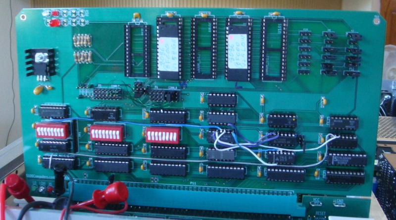
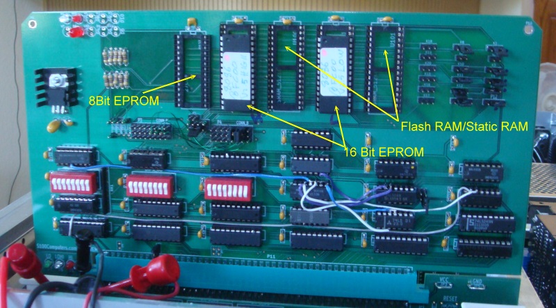
Here is a picture of the prototype board:-
 
  Prototype ROM Board
  
 
Please excuse some of the wire connections. They will be corrected on the final board.

PROM/RAM Pin Jumpers.
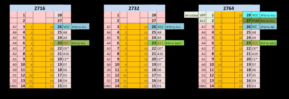
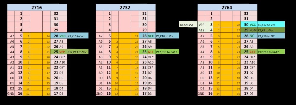
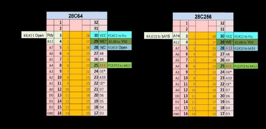
The board will accept numerous 5 Volt EPROM, EEPROM, FLASH and RAM chips.  That's the good news. The only catch is you have to be careful with what jumpers you use for each chip type. Here are the configurations for the most common memory chip types:-

For 8 bit EPROMS that reside in socket U123:-
 
 
Pinouts 8
      
For 16 bit EPROMS that reside in sockets U4 and U121:-
  
Pinouts 16 1
   
Pinouts 16-2
  
Note: All EEPROMS (electrical erasable, rather than UV light) of the equivalent capacity above will have the much the same pinouts/jumpers. However in a few cases where there are differences. For example with 27C256 EPROM's and 28C256 EEPROM's. So always check the pinouts. I made this mistake recently with 28C256 EEPROMS only to have them re-programmed in a 27C256 socket setup!

For 16 bit EE-PROMS that reside in sockets U4 and U121:-
  
EPROM3


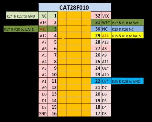
For a pair of 128K X8 FLASH RAM's (16 Bit) in sockets U100 and U101:-
 

Flash RAM
 
Note you do not have to use the full 128K of Flash RAM. By adjusting (see below) the RAM/ROM window that activates 16CS* using SW2 and IC2A you can select sections of the chip and surround the rest with other S-100 RAM on the bus.  The other RAM board however must recognize the S-100 Phantom line (pin 76). The 4MG Static RAM board is an example of this.

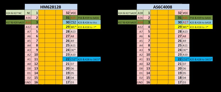
For a pair or Static RAM's (16 bit) in sockets U100 and U101:-
 

Static RAM
 
These two chips will allow the board to have 128KX16 or 512KX16 (or 256KX8 and 1MGX8) of fast static RAM memory on board.  Very useful is the fact that at the same time the board can have an 8 bit EPROM (or EEPROM) for a Z80 board.


ROM Memory Board Logic

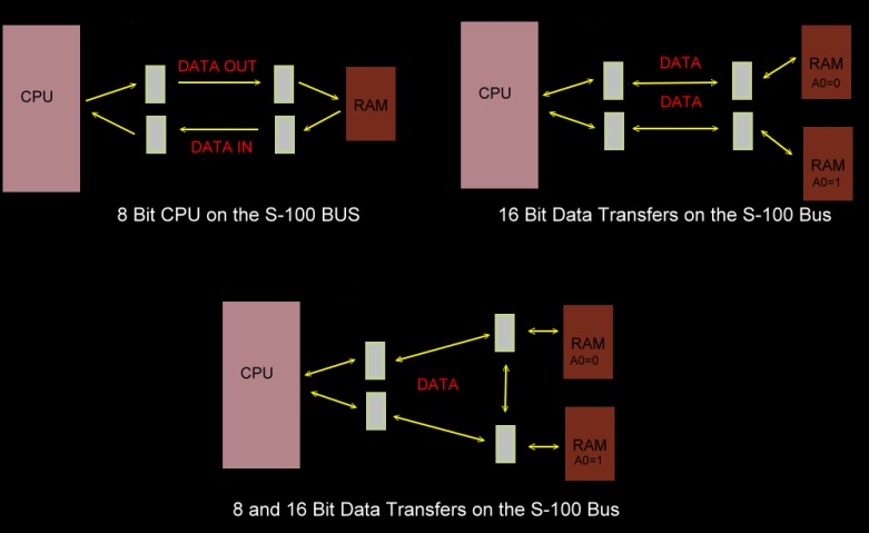
This is a repeat of the discussion on the 4MG RAM Board -- The S-100 bus was designed around the 8080 CPU. This CPU has a bi-directional 8 bit data path, however because Ed Roberts wanted to control it via a series of front panel switches, the CPU data bus was broken out into separate 8 bit Data In and Data Out paths on the S-100 bus.   This worked fine. RAM boards had their RAM chips connected to both data paths and I/O boards were likewise connected.   It was a somewhat inefficient setup but it worked (all for a simpler front panel).   The first diagram below shows the basic layout.
 
8 and 16 bit systems

When 16 bit CPU's came along things got more complicated.  All 16 bit CPU's have a 16 bit bi-directional data path.  They can interface directly to RAM chips that are 16 bits wide or two 8 bit wide RAM chips. In the early 80's the latter type of RAM's were much more common. Two 8 bit wide RAM chips differing only in address line A0 (0 or 1), would be connected to the 16 bit bus.  The S-100 Data In and Data out lines were utilized together as a single bi-directional 16 bit bus and were connected via buffers to the CPUs 16 data line pins.

Now if all you were going to use was such a 16 bit CPU that would be fine. But such a setup would not work with older 8 bit RAM cards or indeed with any I/O cards which also expect a split 8 bit interface.

The solution was simple and elegant and the heart of the IEEE-696 standard. For 16 bit systems the bus behaves as a 16 bit bidirectional bus. For 8 bit systems a bridge buffer on each RAM board transfers the data coming and going to the board over separate 8 bit data lines depending on whether it's address is odd or even. If we have 8 bit data coming to the board on an even address, it travels on the "Data Out" path and goes directly to the A=0 RAM bank.  If instead the 8 bit data is destined for an odd address it arrives as before at the RAM board top buffer but then is dropped down to the lower A0=1 RAM bank  via a bridging buffer.

If the 8 bit CPU wants to read a even address it activates this buffer in the opposite direction so the RAM A=0 bank data is shifted down to the S-100 data in lines. If the 8 bit CPU wishes to read am odd RAM address the A0=1 RAM bank data travels directly to the  CPU on the Data Out bus.

The hardware logic to do this is quite tricky. You need to factor in if we have a CPU read or write, if the data is 8 bits or 16 bits wide and if the destination address is on an even or odd address line.  (Fortunately no common 16 bit CPU transfers 16 bit data an odd address line).

Now back in the mid 80's companies like CompuPro and Macrotech implemented this logic in ROM like chips called
PAL's. Unfortunately they never published the code.  


The Circuit
I wanted to build a S-100 PROM board that would serve me well into the future. Where I could use it with very fast and wide CPU's. I wanted to stick with DIP type chips. There are higher density PROM chips than the 512K/chips we use here but many require SMT. These are difficult to work with.   I have had good success with the 32 Pin DIP Alliance AS6C4008 (512KX8 Static RAM) chips, (Jameco Part #1927617) with the 4MG Static RAM Board. I wanted to be able to use this chip again here.

The board utilizes 74LS682's for RAM addressing. If your are unfamiliar with this technique click here.

The hardest part was figuring out a
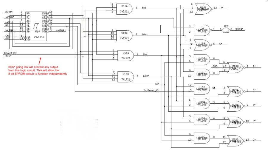
PAL equivalent circuit using standard TTL chips. I came up with the following "7400" TTL layout.  It takes a few chips as opposed to a single PAL chip, but it is fast and reliable.

PAL circuit

This PROM board is really three boards in one. It's an 8 bit EPROM board for an EPROM that resides in < 64K of the S-100 bus address space and two 8 or 16 bit EPROM/RAM boards for any address from 0 to 16MG.   The former is for use with 8080/Z80 CPU's. Very useful is the fact that both sections can reside together and overlap on the board. A typical application might be CPM3 and/or CPM with a memory disk. Note however, these applications require a CPU board that can address above 64K (Intersystem's, Compupro etc).  The board can accommodate up to 1MG of 8 bit RAM.  Remember also, that to program EPROMs for 16 bit CPU's you have to program the "Low Byte" in one EPROM and the "High Byte" separately in the other EPROM pair.
  
  Board layout

 
The board has three independent buffers to place data on the S-100 bus. These are controlled separately by three signals 16CSA*, 16CSB* and 8CS*. The circuit is arranged so both the board data output buffers/EPROMS cannot come on together.

Finally you will notice for the CAT28F010 FLASH RAM's (Jameco Part #242608), the CE* is tied to ground (rather than 16CSB*).  The reason for this is that these Flash RAM's go into a "Low Power Mode" when CE* is high. There is a latency time required for the chip to "warm up" after CE is brought low. Keeping it low avoids the problem. The chips are low power anyway!  This unfortunately does mean that FLASH RAM chips cannot be used at the same time as EPROM's in the U4 & U121 sockets. 

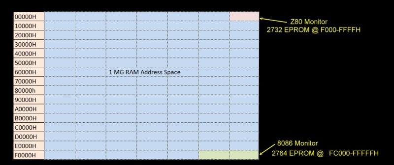
A typical layout of a board in a Z80/8086 dual CPU system might look like this:-
 
Memory map
 
The boot Z80 monitor EPROM/EEPROM would reside at F000H in RAM.  With a Z80 CPU board like the Intersystem's board, the rest of memory could be used for CPM3 banks and/or as a memory disk.  This is what I do in my system. If a 8086 CPU has control of the bus  then it will first start from the reset address FFFF0H in RAM. Here it would find the end of the 8086 Monitor (in a pair of 28C64 EEPROMS). From there it would jump to the start of that monitor (at FC000H). Amongst the commands would be one to boot CPM86.  Again this is the way my system is setup and I will describe all this later when we do a 8086 S-100 CPU board.

There are two things to keep in mind with the above arrangement. First, the static RAM 512X8 pair occupy the entire 1MG address space. The circuitry on the board insures that these RAM chips are not activated if any of the above 3 EPROMS are addressed.   See below.

For the 8 bit EPROM at F000H-FFFFH, if it is addressed, the line 8CS* will go low. This inactivates any output from the
PAL like circuit. Instead it activates its own S-100 bus buffer (U125).

For the 16 bit EPROMs at FC000H-FFFFFH, they are addressed by 16CSA* going low. This same line is inverted  (U14B) and used to inhibit 16CSB* (U124D) which normally activates the static RAM chip pair (U100,U101).

One final thing, we normally don't want the Z80 EPROM to be active when the 8086 CPU is controlling the bus.  The 8086 gets control of the bus when the S-100 signal TMA0 signal goes low.  Again look at the schematic, by jumpering K29 1-2 and connecting P19, pin 7 to P21 pin 7 and opening SW4,7 we can insure that this EPROM is never active when the 8086 has control of the bus.  Much of this may sound confusing right now. It will become clearer when we do 16 bit CPU boards next year.

 
The Final EPROM S-100 Board
The above board had worked without any problems in two systems using CPM+ and CPM86 with a verity of hardware configurations so Andrew and I decided to go ahead and do a final commercial type board.  The trace layout was optimized further before doing this. 

Here is a schematic and detailed layout of the board. 
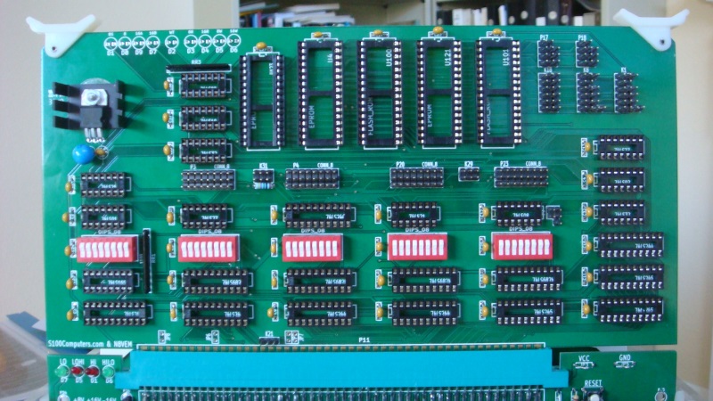
Here is a picture of the final Board:-

Final PROM Board
You can see that it includes some changes form the above prototype board.   It is now really three boards in one.  The 8 bit EPROM socket has its own self contained circuitry and addressing capability.  The 16 bit EPROM/EEPROM section is also separated from the RAM/Flash RAM circuit.

Building the Board
This board can accommodate almost any type of common EPROM or EEPROM, quite a few static RAM chips and also Flash RAM chips.  That's the good news, the bad news is that there are quite a few jumpers and switch settings  you need to setup to configure the board for your setup.  In building this board, sure you could install everything set up all jumpers at once and plug it into your system and in theory have it come up the first time. If you take this approach -- also buy a lottery ticket.  Better to step the build in a series of steps. Checking functionality as you go along.  Here is a guide to doing this.

First install all non-IC components on the board -- including the 5V (1.5A) voltage regulator.  On the latter, I have inserted a mica washer between the heat sink and the board because one of the traces on the front side runs a little close to the heat sink.  Probably overkill, but check this out. Insert the board into your system and check your system boots up fine.
 

Empty Board

First we will install the 8 bit EPROM circuitry. We start by adding in the chip select addressing circuit.  Layout the board circuit in front of you. This will make things clearer as you go along. Install U3, U20, U21, U8, U11, U14 and IC3A.  Next we have to decide where we will place our EPROM in the Z80's 64K address space.  We do not want your RAM board and this EPROM board putting data on the bus at the same address. If your current systems RAM board accepts the phantom line (S-100 pin 67) things are simple. The phantom signal from this board  (K7 pin1) will in-activate your RAM board when EPROM on this board is addressed.  If your RAM board does not recognize the phantom signal (most do), you need to select a < 64K RAM board and place the active adders range of this board outside that space.  For example a 32K RAM board and place the EPROM at 8000H for this board.

In our demo example we will place a 2732 EPROM at 8000H in memory. We need therefore to configure the 74LS682 IC3A such that pin 19 of IC3A goes low if the Z80 addresses RAM from 8000H to 8FFFH.  So if we place in RAM at 0H the following code:-
 
3A 00 80    ; LD    A,(8000H)
C3 00 00    ; JP     0000H


The Z80 will continuously read memory at 8000H in the EEPROM.  Please see here to understand how 74LS682 addressing is done.   For addresses in the range 8000H to 8FFFH, A15 will always be high and  A14, A13, and A12 will always be low.  So we jumper P19 and P21 as follows:- 1-1, 2-2, 3-3, 4-4. Since we are using 4K we ignore A11 so tie p21,5 to P20. We also ignore the phantom INPUT, so also P21,6 to P20 (and P21,7 to P20), but do accept the low going pulse from U14 pin 12 when S-100 addresses are < 64K (so P19 pin 8 to P21 pin 8).  
On SW4 then 1-8 are:-  open,closed,closed,closed,  closed,closed,closed, closed.

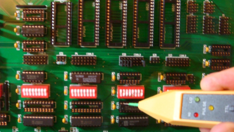
Setup the board as described above and check with a logic probe for a low going pulse on IC3A pin 19.
 
CS on IC3A
  
Next add U124 and U1. Check as above for a low going pulse on pin 3 of U124.  You can then install LED's  D1 and D8.  They should light up with the above continuous software loop. 

Next install U2 (but bend out pin 4 for now). Jumper K7, 1-2. 
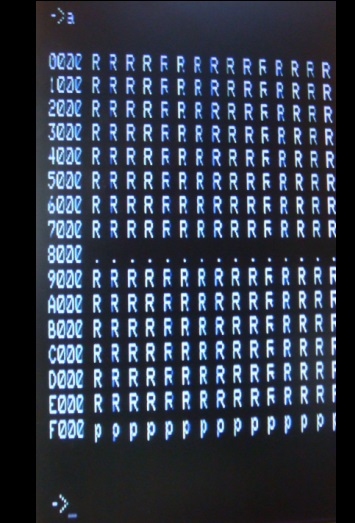
If you have a Z80 monitor that displays a memory map you should see no RAM are 8000H to 8FFFH. 
Something like this:-
 
memory map
 
Next install U10 and  U125. Check pins 1 & 19 of U125 pulse low with the above software loop.
 
We will now install a 2732 EPROM.   Consult the pinout diagram above for this EPROM.   Jumper K22, 2-3 and K31, 2-3.   You now should be able to display the code in the EPROM and if necessary jump to it.   Any time you want to inactivate this circuit  (i.e.. make the EPROM invisible on the board) close switch 7 of SW4.

16 Bit Circuitry
New we will install the more complex 16 bit circuitry and/or > 64 K addressing for EPROMS and RAM.  Initially we will use 28C64A EEPROMS as an example.   This is where things get a little bit more complicated.  You will need some way of addressing >64K in the S-100 Bus.  If you have a 8086 CPU board in your system already this is no problem.  Alternatively you can use a Z80 board that can address > 64K like the one I use and describe here (and hopefully soon will be available).   I will be doing 16 bit CPUs next year, so you may wish to wait until then for this feature.

In our initial setup we will place the 28C64 EEPROM at 8C000H in RAM.   This will avoid its interfering with a 8086 Monitor normally at FC000H in RAM . On reset the 8086 will jump to this monitor.

Install IC1, IC4A and U14.  Since we are addressing RAM at 8C000H, address lines A23-A20 are low, A19 is high, A18-A16 are low on P1 as inputs to IC1. Match SW1 accordingly. For P22, A15 and A14 are high, A13-A11 are ignored, pin 8 of P22 will be low. Match SW5 accordingly.

Display memory at 8C000H (either with your 8086 monitor or with a Z80 that can memory map).  Exactly as above,  pin 6 of U124 should pulse low.  Next install all IC on the board EXCEPT the EEPROMS,  U22, U23 and U24.  You can also bend in pin 4 of U2.  Insert the board into your systems and check it does not hang.  Next install U22,U23, and U24. Repeat the above check.

We are now ready to install the 28C64 EEPROMS.  Carefully consult the pinout requirements of the chip. See the above diagrams on this page.  Remember the data sheet pinout numbers are different from the board socket numbers on this board (unless you are using 32 pin chips).

For 28C64A's the jumpers are as follows:-
Odd Byte EEPROM:- K1 2-3,   K4 2-3,   K5 1-2   P12 2-3.     Even Byte EEPROM:-   K8 2-3,   K11 2-3,  K12 1-2,  P13 2-3.

Switch Settings
 

Once you have confirmed the EEPROM is working fine you can relocate to a more useful location. In my case I have my 8086 monitor in two 28C64A EEPROMS at FC000H to FFFFFH.   After an 8086 reset the CPU jumps to FFFF0H in this EEPROM and from there to the start of the monitor at FC000H.  The switch settings for a pair or 28C64's at this location are:-

SW1  close, close, close, close, open, open, open, open.,    Jumper all P1 pins to corresponding P5 pins
SW5  open, open, open, open, open, open, open, close.,    Jumper (only) P22 pins 1, 2 & 8  to  P24 pin 1, 2 & 8


[BTW, more recent versions of my 8086 Monitor require 28C256 EEPROMS . In these versions half of the EEPROM is used, the 8086 Monitor starts ate F8000H.  See here. ]

Up to 8 wait states can be added to any CPU read/write cycle with this board. Switch SW3 controls the number of wait states. If all switches are open, no wait states are added. SW3-1 closed, adds one wait state,  SW3-2 closed adds 2 wait states... etc.  For a 8MHz 8086 I typically use two wait states for most ROMS. You can probably get away with one but why risk it. 

Remember switches are close right to left. (One wait state is the right most switch, eight wait states, all 8 switches are closed). Do not use other switch patterns.

Note there is one small error in the layout of this board. LED D2 is used to indicate wait states. Unfortunately it is on in the absence of wait states going off if a wait state is added. It really should be the other way around.  This is easily corrected by bending out pin 9 of U17 and on the back of the board jumpering pin 9 of U17 to pin 7 of U17.

Adding Static RAM to the Board
Now lets add some static RAM to the board. Again there are a number of available RAM chips and many permutations and combinations as to how things can be configured.   There are two basic ways RAM can be added to this board.

One is along side the EEPROM/ROMs.  SW1 sets the starting and ending location of the RAM block and within this block the EEPROM/ROM resides.  The relative location of the ROM's within the total RAM space is set by SW5.   Not all of the space defined by SW1 need be used by RAM. The switch SW2 allows one to block out or include sections.

Alternatively the board can be configured as an (up to) 1MG Static RAM board. 16 bit ROM's are not utilized, however the 8 bit ROM capability remains. A typical application here might be CPM+ and a memory disk with a Z80 Monitor/Boot BIOS at F000H.  You can even splice in a 16 bit EEPROM/ROM pair in this 1MG static RAM by jumpering connections between P1 and P24.  However this is really not optimum because the onboard RAM is slowed down to the access speed of the EEPROM/ROM. A better approach is to utilize our dedicated 4MG Static RAM Board and this board as a dedicated EEPROM/ROM board.

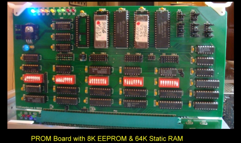
As an RAM example, lets pick 128K X 8 chips (HM628128LP-7).  We will place these chips along side the EEPROMS and put them in sockets U100 and U101.   Lets start the RAM at F0000H. It will therefore reside at F0000H to FFFFFH. We will puncture this RAM space with an EEPROM at FC000H to FFFFFH.

128K Static RAM
  
Note: These RAM chips are way overkill for this example since we are only using 64K of the total 128K X 2 bytes available. The extra RAM is simply ignored by the board circuitry in this example. The above picture shows the board setup.

For the HM628128LP static RAM chips the jumpers are as follows:-
Odd Byte RAM:- K17 1-2,   K25 1-2,   K15 2-3,  K23 2-3,     Even Byte RAM:-  K20 1-2,  K28 1-2,  K18 2,3  K19 1-2,  K26  2-3.

Since we want to include all RAM from F0000H to FFFFFH, no connections on P2 to P6 are made except P2-8 to P6-8.  All connections on SW2 are open except SW2-8 which is closed/ground.  Here is an 8086 Monitor Memory Map picture of the board:-

RAM 8086 Memory Map


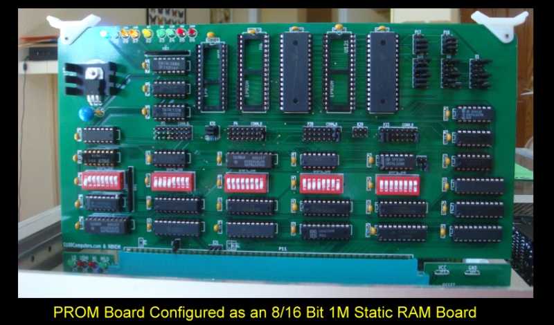
As another example lets configure the board as a simple 1MG Static RAM board that will work in 8 or 16 bit mode.   In this case we use AS6C4008 512K Static RAM chips.  Two of them. Here is a picture of the board with this setup:-
 
1MG Static RAM
 
Again we need to carefully configure the appropriate jumpers for the RAM pins.

For the AS6C4008 static RAM chips the jumpers are as follows:-
Odd Byte RAM:- K17 1-2,   K25 1-2,   K15 2-3,  K23
1-2 K24 1-2.    Even Byte RAM:-  K20 1-2,  K28 1-2,  K18 2,3  K19 1-2,  K26 1-2   K27 1-2.

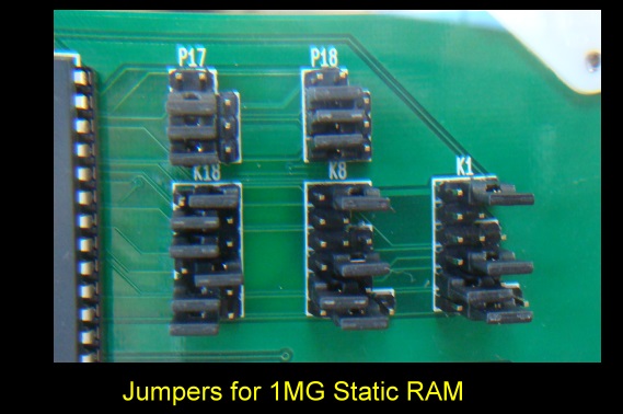
Since we will be using the first 1MG of the S-100's 16MG address space the only jumpers on P1 to P5 are A23, A22, A21 and A20. The rest are removed.  On SW1 switches 1, 2, 3 & 4 are closed/ground and 5, 6, 7 and 8 are open.  The only jumper on P2 to P5 is 8-8 and the only closed switch on SW2 is number 8.  Finally to inactivate the 16CSA* circuit,  remove jumper P22 to P24 8-8 and close SW5 switch 8.  I know this may all sound confusing but if you look at the schematic and understand how 74LS682 address selection works it becomes quite easy.
 
Here is a close-up picture of the jumpers:-
 
1MG Static RAM
 
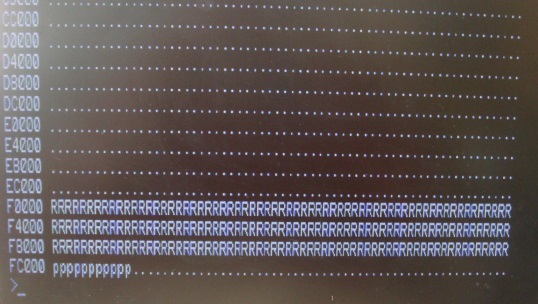
Here is a memory map display using my 8086 Monitor:-


I will leave it as an exercise for the reader to figure out how to splice in an 8K EEPROM at the top of this memory space -- for example an 8086 Monitor at FC000H.  (Hint, use wire wrap jumpers from connector P1 to P24).

Finally the board can be configured to accommodate Flash RAM chips. These behave essentially the same way as the above RAM chips.  The only difference as I said above is that the board cannot accommodate a 16 Bit Flash RAM and a 16 bit EEPROM at the same time. (8 bit EPROMS are fine). 

BTW, it may be possible to actually program Flash RAM's on this board. I have not looked into this.  I have always programmed my Flash RAMs separately on a Wellon VP-280 programmer using PC software.


Version 02 of This Board.
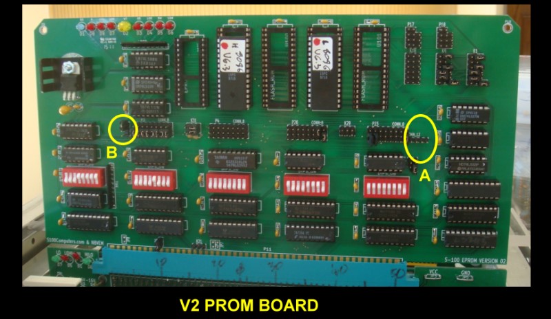
The above board proved very popular. All production quality boards were quickly take.  A second "V2" version of the board has now been made. Some very minor updates were made to the above board and are incorporated in boards that have "S-100 EPROM VERSION 02" at the bottom right hand corner of the board.  These minor changes are:-
 
1 Connect BOARD_WAIT to pin 7 of U17 (instead of pin 9).
2 Have a jumper at pin 8 of U2C  that can go to either pin 9 of U2c or pin 11 of U124B, 16CSB* 
(this eliminates wait states if RAM is used). (Jumper B below)
.
  3 Bring out A16, A17, A18 and A19 as extra jumper contacts at P22. (Jumpers A below)
This allows an EPROM at FC000H if 1MG static RAM is present at 0000H. 
For the V1 board, we needed wires from P1 to p24.
 
      
V2 Board
       

A Production S-100 Board.
Realizing that a number of people might want to utilize a board like this together with Andrew Lynch at N8VEM (see here) we have completed a second run of these boards. If you have an interest in such a bare board, let Andrew  know via e-mail at:-  lynchaj@yahoo.com

 
Please note all the above clearly applies only to people who know what they are doing and can  do a little soldering and board assembly.  There will be little hand holding at this stage.

Update
I come back to using this board from time to time,  when I am debugging multiprocessor systems.    While the board will accept almost any type of PROM, I have to admit configuring it for the appropriate ROM is quite a challenge.   You really have to carefully study the PROM pinouts and sit down an carefully configure the boards address decoding.   Remember it is three boards in one.  However most of the time you will be concerned with EPROMS and the SW5/16CSA* section. The other two sections can be ignored/inactivated.

As time goes by I will show pictures of exact configurations I use to help you get started.  Please note the number of wait states  will vary depending on your S-100 bus (and whether you have the card in an S-100 bus extender board slot). Start with a high number and work down.


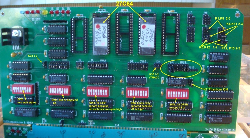
Example 1: Two 27C64 (UV Erasable) E-PROMS (16 bit mode) at address 8C000H to 8FFFFH.
  

Config 27C64

  
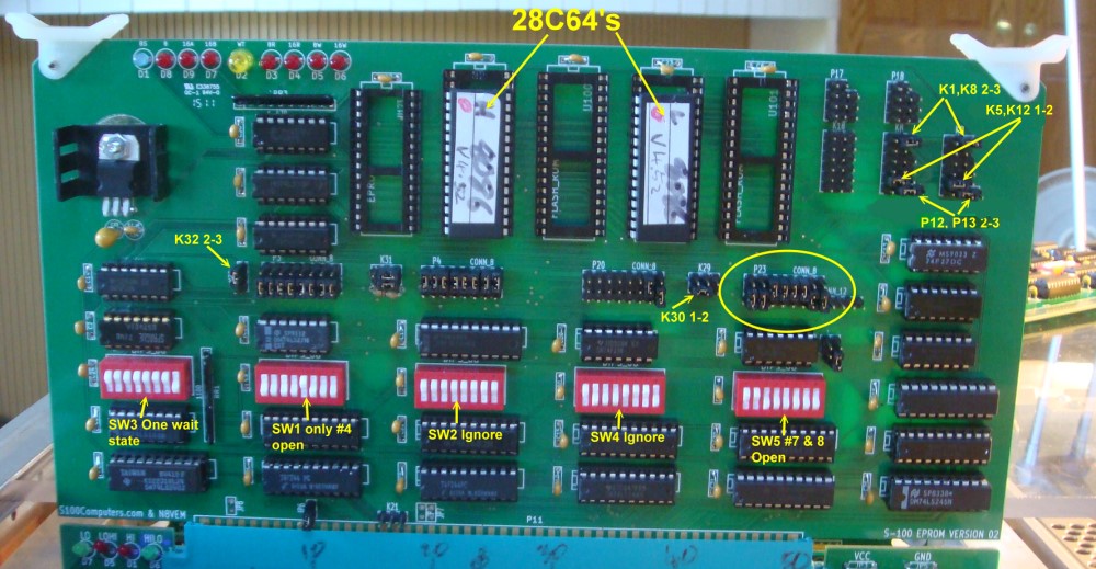
Example 2: Two 28C64 (Electric Erasable) EE-PROMS (16 bit mode) at address 8C000H to 8FFFFH.
  

Config 28C64

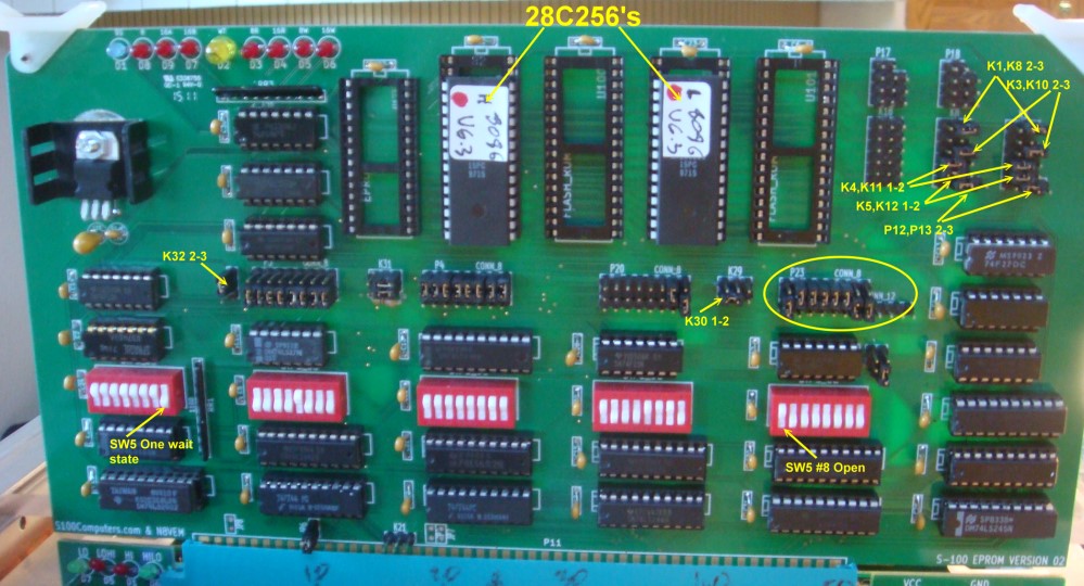
Example 3: Two 28C256 (Electric Erasable) EE-PROMS (16 bit mode) at address 88000H to 8FFFFH.

Confif 28C256

In the case of the 28C256's I am only using half of the total EEPROM's capacity, (the top half).  If you wanted the whole EEPROM
(i.e. 80000H to 8FFFFH) you would jumper  P23-1 to P24-1 and close SW5 #8.

Please not I have found these EE-PROMS (ATMEL AT28C64's, Jameco #276752 , or  AT28C256's , Jameco #74843)  to be particularly sensitive to read access times. They seem to require at least one wait state, even at 8MHz . To run the board with our 8086 board set to 10MHz, the following 74LSx chips need to be changed to 74Fxx types:- U15, U18, U13, U19, U25.  

Always check you system, by copying the EPROM memory to another place in RAM and verifying the move, (the 8086 Monitor "M" and "V" commands).  If you want long term high speed reliability, I recommend the UV erasable 27XXX EPROMS.

Wait States on the 8086 Board
Note to use  this board's E-PROMS (and EE-PROMS) instead of the onboard EPROMS on the 8086 board to bring up the 8086 Monitor it is important that the EPROM wait state(s) jumper on the 8086 board is removed (a jumper on any one of the p65 pins); as well as  of course inactivating its onboard EEPROMS by jumper K3 2-3.   With this arrangement (using 74Fxx chips above), the board will work at up to 10MHz on the S-100 bus with 6 wait states using 27C128 EEPROMS for example.  

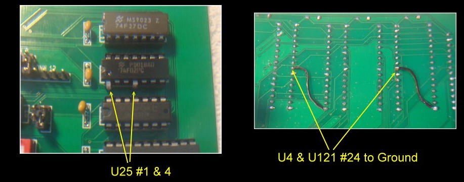
You can reduce the above wait state requirement by at least two wait states by grounding the OE* pins of the EPROMS.  The picture below shows the configuration.

Eliminate Wait States
Bend out pins 1 & 4 of U25. Connect the OE* pins of the E-PROMs to ground. This pin will vary, depending on the EPROM type.   This modification gives the EPROM extra time to place its data on the inputs of the 74LS245 bus drivers. A jumper like this should have been (and will be) on the next run of boards -- if there is one.   The D* and E* (see the schematic) signals are only high for static RAM writes.

BTW, the 8086 board requires no wait states at 10MHz if EEPROM's are used locally on the CPU board itself; however this is really pushing it. Normally I have one EEPROM wait state for reliability. 

The links below will contain the most recent schematic of this board.
Note, it may change over time and some IC part or pin numbers may not correlate exactly with the text in the article above.
 

MOST CURRENT EPROM BOARD SCHEMATIC
(V2, FINAL, 8/21/2010)
MOST CURRENT EPROM BOARD LAYOUT 
(V2, FINAL, 8/21/2010)
MOST CURRENT PARTS LIST   (V3.1, FINAL, 9/26/2011)
MOST CURRENT EPROM BOARD V2 SCHEMATIC (V3.1, FINAL, 9/6/2011)


Other pages describing my S-100 hardware and software.
Please click here to continue...


This page was last modified on 09/26/2011